97
9140CINDCO02/10
ATA8741
ture is similar to the OC0A toggle in CTC mode, except the double buffer feature of the Output
Compare unit is enabled in the fast PWM mode.
20.7.4
Phase Correct PWM Mode
The phase correct PWM mode (WGM02:0 = 1 or 5) provides a high resolution phase correct
PWM waveform generation option. The phase correct PWM mode is based on a dual-slope
operation. The counter counts repeatedly from BOTTOM to TOP and then from TOP to BOT-
TOM. TOP is defined as 0xFF when WGM2:0 = 1, and OCR0A when WGM2:0 = 5. In
non-inverting Compare Output mode, the Output Compare (OC0x) is cleared on the Compare
Match between TCNT0 and OCR0x while upcounting, and set on the Compare Match while
down-counting. In inverting Output Compare mode, the operation is inverted. The dual-slope
operation has lower maximum operation frequency than single slope operation. However, due to
the symmetric feature of the dual-slope PWM modes, these modes are preferred for motor con-
trol applications.
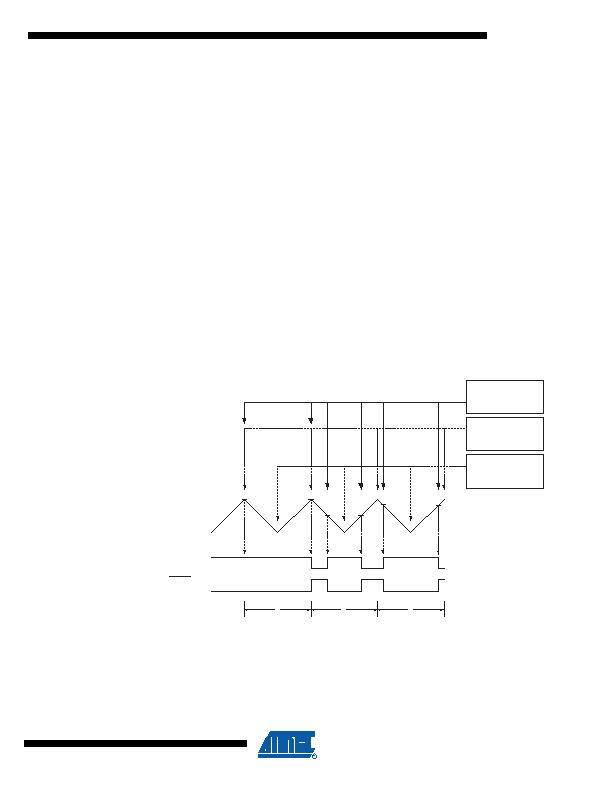
In phase correct PWM mode the counter is incremented until the counter value matches TOP.
When the counter reaches TOP, it changes the count direction. The TCNT0 value will be equal
to TOP for one timer clock cycle. The timing diagram for the phase correct PWM mode is shown
on Figure 20-7 on page 97. The TCNT0 value is in the timing diagram shown as a histogram for
illustrating the dual-slope operation. The diagram includes non-inverted and inverted PWM out-
puts. The small horizontal line marks on the TCNT0 slopes represent Compare Matches
between OCR0x and TCNT0.
Figure 20-7. Phase Correct PWM Mode, Timing Diagram
The Timer/Counter Overflow Flag (TOV0) is set each time the counter reaches BOTTOM. The
Interrupt Flag can be used to generate an interrupt each time the counter reaches the BOTTOM
value.
In phase correct PWM mode, the compare unit allows generation of PWM waveforms on the
OC0x pins. Setting the COM0x1:0 bits to two will produce a non-inverted PWM. An inverted
PWM output can be generated by setting the COM0x1:0 to three: Setting the COM0A0 bits to
TOVn Interrupt Flag Set
OCnx Interrupt Flag Set
1
2
3
CNTn
eriod
Cn
Cn
(COMnx1:0 = 2)
(COMnx1:0 = 3)
OCRnx Update
发布紧急采购,3分钟左右您将得到回复。
相关PDF资料
ATA8742-PXQW
MCU W/TRANSMITTER ASK/FSK 24QFN
ATA8743-PXQW
MCU W/TRANSMITTER ASK/FSK 24QFN
ATAVRRZ200
KIT DEMO AT86RF230
AV101-12LF
ATTENUATOR HIP3 0.70-1GHZ 8-SOIC
AV102-12LF
ATTENUATOR HIP3 1.7-2GHZ 8SOIC
AV113-12LF
ATTENUATOR HIP3 2.1-2.3GHZ 8SOIC
AXUV100G
SENSOR ELECTRON DETECTION
B0205F50200AHF
XFRMR BALUN RF 200-500MHZ 1608
相关代理商/技术参数
ATA8742
制造商:ATMEL 制造商全称:ATMEL Corporation 功能描述:Microcontroller with UHF ASK/FSK Transmitter
ATA8742C- PXQW
制造商:Atmel Corporation 功能描述:Embedded C incl RF Tx for 433 MHz
ATA8742C-PXQW
功能描述:8位微控制器 -MCU RoHS:否 制造商:Silicon Labs 核心:8051 处理器系列:C8051F39x 数据总线宽度:8 bit 最大时钟频率:50 MHz 程序存储器大小:16 KB 数据 RAM 大小:1 KB 片上 ADC:Yes 工作电源电压:1.8 V to 3.6 V 工作温度范围:- 40 C to + 105 C 封装 / 箱体:QFN-20 安装风格:SMD/SMT
ATA8742C-PXQW-1
功能描述:EMBEDDED INCL RF TX FOR 433 MHZ 制造商:microchip technology 系列:- 包装:剪切带(CT) 零件状态:在售 频率:429MHz ~ 439MHz 应用:通用 调制或协议:UHF 数据速率(最大值):32kbps 功率 - 输出:7.5dBm 电流 - 传输:9.8mA 数据接口:SPI 天线连接器:PCB,表面贴装 存储容量:4kB 闪存,256B EEPROM,256B SRAM 特性:- 电压 - 电源:2 V ~ 4 V 工作温度:-40°C ~ 85°C 封装/外壳:24-VQFN 裸露焊盘 标准包装:1
ATA8742-PXQW
功能描述:8位微控制器 -MCU Embedded uC incl RF Tx for 433 MHz
RoHS:否 制造商:Silicon Labs 核心:8051 处理器系列:C8051F39x 数据总线宽度:8 bit 最大时钟频率:50 MHz 程序存储器大小:16 KB 数据 RAM 大小:1 KB 片上 ADC:Yes 工作电源电压:1.8 V to 3.6 V 工作温度范围:- 40 C to + 105 C 封装 / 箱体:QFN-20 安装风格:SMD/SMT
ATA8743
制造商:ATMEL 制造商全称:ATMEL Corporation 功能描述:Microcontroller with UHF ASK/FSK Transmitter
ATA8743C- PXQW
功能描述:8位微控制器 -MCU Embedded uC incl RF Tx for 315 MHz
RoHS:否 制造商:Silicon Labs 核心:8051 处理器系列:C8051F39x 数据总线宽度:8 bit 最大时钟频率:50 MHz 程序存储器大小:16 KB 数据 RAM 大小:1 KB 片上 ADC:Yes 工作电源电压:1.8 V to 3.6 V 工作温度范围:- 40 C to + 105 C 封装 / 箱体:QFN-20 安装风格:SMD/SMT
ATA8743C-PXQW
制造商:Atmel Corporation 功能描述:EMBEDDED ?C INCL RF TX FOR 868 MHZ - Trays 制造商:Atmel Corporation 功能描述:EMBEDDED C INCL 868MHZ TX